
The Bode/Nyquist Plot applet now has a tab for impulse and step function responses. As in previous versions the focus remains on design of cascaded filter sections, so numerator and denominator are still entered as one or more polynomials, which get multiplied and terms collected before plotting. For discrete time investigations, try my new Z-Domain Bode/Nyquist Plot Java applet.

|
|
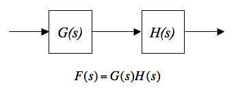
In general, the transfer function of any linear system can be expressed as a ratio of two polynomials in powers of the Laplace variable s. The order of the transfer function is just the difference between the highest and lowest powers of s present. The general form shown above has powers ranging from zero to two, so the form shown is 2nd order. When two filter sections are cascaded, as with G(s) and H(s) above, the overall transfer function F(s) is the complex product of the two individual transfer functions. The steady-state gain for a continuous wave (CW) input is the absolute value of the transfer function, evaluated by setting s = jω where j is the square root of -1 and ω is the angular frequency of the input in units of radians/second. The phase shift for the same CW input is the argument (arctangent) of the transfer function at that frequency. The Bode Diagram gives a log-log plot of gain and a lin-log plot of phase, so the product of two transfer functions can be visualized by simply summing up the values. Following are some details of how to use the Bode/Nyquist Java Applet.
While developing the applet I kept in mind this short list of simple test cases with known results, which allowed me to quickly verify that the applet actually works. Type the numerator and denominator strings into the applet's entry fields and click "Plot Response" to see the result. Corner or center frequency ω0 in each case is 1 radian/second, or about 0.1592 Hz. These sections can be cascaded in combination, and scaled in amplitude or frequency for further tests. Diagnostic information is sent to the Java Console to help you better understand the applet's operation.
| Description | Numerator | Denominator | Notes |
|---|---|---|---|
| Integrator | (1) | (1,0) | Unity gain at ω0, constant phase of -90° |
| Differentiator | (1,0) | (1) | Unity gain at ω0, constant phase of +90° |
| 2nd order low pass | (1) | (1,1.414,1) | -3 dB gain at ω0, phase crosses -90° at ω0 |
| Bandpass filter | (1,0) | (1,.25,1) | +12 dB gain at ω0, phase crosses 0° at ω0 |
| 2nd order high pass | (1,0,0) | (1,1.414,1) | -3 dB gain at ω0, phase crosses +90° at ω0 |
| Notch filter | (1,0,1) | (1,1,1) | Notch centered at ω0, phase flips from -90 to +90° at ω0 |
| 2nd order phase shift | (1,-1,1) | (1,1,1) | Unity gain at all frequencies, phase crosses 180° at ω0 |
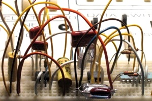
The real utility of this applet isn't in matching well-known textbook cases, but in accurately predicting the performance of actual filters that you design and build. To that end, I've studied two simple design examples shown below, taken from the world of real-time audio analyzers (RTAs). Both examples use cascaded filter sections to build up complicated transfer functions. In each case, output from the Bode/Nyquist applet closely matches measured results obtained on my bench with a simple breadboard. Unless otherwise noted, all opamps are Texas Instruments TLC2272CP (operating with filtered, regulated +/- 5 Volt supplies), all resistors are 5% 1/4 Watt carbon film (in series or parallel combination of at most 2 resistors, to get close to desired value), and all capacitors are polypropylene film, Panasonic P-Series (2% tolerance at nominal value).
A real-time analyzer operates by separating its input into discrete channels and showing each channel's amplitude separately. An octave-band analyzer, for instance, might separate its input into ten octave-wide channels with center frequencies ranging from 32 Hz to 16 kHz. Here we consider the 1 kHz filter response which will be fourth order to reject adjacent channel signals, and will be peaked at two frequencies with an offset to flatten response within the passband. The slight dip at the center frequency is a design tradeoff that can be varied to meet your needs.
|
|
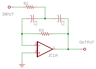
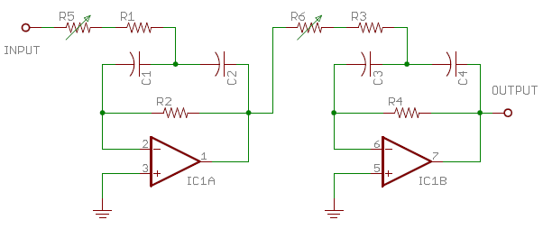
As Don Lancaster describes in his "Active Filter Cookbook" (Lancaster [1995]) the two-pole fourth-order bandpass response is well-suited for implementing a flat-top bandpass filter. Following his design process, we set the staggering factor a = 4/3, or about 1.333, and Q = 2.5. This will leave us with a -0.5 dB dip at the center frequency, which is quite reasonable for use in a real time analyzer. We'll cascade two sections of the type shown in Fig. 2 above, which is a single-amplifier multiple-feedback bandpass filter. Starting with all component values set to unity (1 Ω and 1 Farad), the center frequency will be 1 radian/second. First I'll change the capacitors to a more practical value of 0.01 μF, which causes a corresponding change in center frequency to 108 rad/sec., or about 15.92 MHz. Both capacitors maintain the same value in this design. Next I change both resistors to 15.92 kΩ to drop the center frequency back to 1 kHz. Then, following Lancaster's recipe, I decrease the input resistor R1 by a factor of 1/(2Q) to 3184 Ω, and increase the feedback resistor R2 by a factor of 2Q to 79.6 kΩ. Finally, I multiply both resistors by a to get the lower section values, and divide both resistors by a to get the upper section values. The results of all this figuring are shown in the table below.
| Lower Section (f0 = 750 Hz) | Upper Section (f0 = 1333 Hz) | |
|---|---|---|
| Resistors | R1 = 4245 Ω, R2 = 106.1 kΩ | R3 = 2388 Ω, R4 = 59.7 kΩ |
| Capacitors | C1 = C2 = 0.01 μF | C3 = C4 = 0.01 μF |
| Numerators | (-23560,0) | (-41880,0) |
| Denominators | (1,1885,22200000) | (1,3350,70140000) |
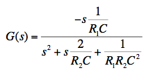
Plugging the parts values given above into the transfer function of Fig. 2, we obtain the transfer function coefficients, shown rounded to 4 significant figures in Table 2 above. Entering the numerator and denominator coefficients into the Bode/Nyquist applet and setting the start frequency to 10 Hz (already done for you in the HTML above), we find the desired flat-top peak response. In addition, we see that overall phase crosses zero at exactly 1 kHz, hits +90° at 707 Hz, and -90° at 1414 Hz. For use in a real-time analyzer one would want the peak gain to be unity, but here we actually have excess gain of about 34 dB over the two filter sections. A simple resistive attenuator (not shown here) in front of each section could return overall gain to unity. Note that the output impedance of the resistive attenuator would have to be accounted for as part of the input resistors R1 and R3.
|
The order in which we cascade the sections has no effect on overall frequency response so we can arrange them to best suit our needs. In this case I've placed the lower section first because it has a higher input impedance. I added the trimmers R5 and R6 (each 1 kΩ, and I reduced R1 and R3 by 500 Ω each) to my breadboard so I could independently adjust the center frequency of each section while accounting for any source impedance seen at the inputs. Unless you are driving the filter with a stiff voltage source and buy precision components for each value, you'll want to align the filter to get the desired response. The procedure is quite easy due to the cascaded design. The input and output of each section can be directly probed to check relative phase shift across the section. Apply a continuous wave (CW) source to the overall input at the desired center frequency for each section one at a time, and adjust the appropriate input resistor (R5 or R6) to get exactly 180° of phase shift across the section you are aligning. You can watch the input and output in a Lissajous pattern on an X-Y oscilloscope, and trim the section's input resistor until the oval-shaped pattern closes to a straight diagonal line. Calibrate your scope probes if appropriate by connecting both X and Y probes to the same circuit node and verifying that the trace is a straight diagonal line. Once each of the sections is tuned to its desired center frequency, everything else will fall into place with measured response matching the calculated response within a fraction of a dB.
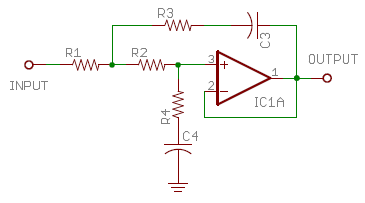
Also from the realm of real-time-analyzers (RTAs), the pinking filter is used to turn white noise from a Gaussian source (equal energy per Hz) into pink noise (equal energy per octave) suitable for studying room acoustics in a real-time measurement. Assuming we have an ideal white noise source, perhaps a maximum-length-sequence (MLS) pseudo-random number generator, we will need a filter with a slope of exactly -10 dB/decade (approx. -3 dB/8va) over three decades of frequency from 20 Hz to 20 kHz. The problem is that traditional filter sections all come with slopes in multiples of 6 dB/8va. The technique I'll use here is to take a standard Sallen-Key (Sallen and Key [1955]) low pass section with a slope of -12 dB/8va and relax its characteristics until the slope is just -3 dB/8va over about two decades of frequency.
|

|
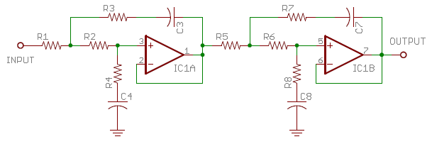
This is done by shifting the capacitor values around, and adding resistors R3 and R4 in series with them. A second section of the same type is then added with its frequency range shifted up by two decades. After tweaking some component values, the smooth merged response shown above is obtained. Ideal component values, which reduce deviation to less than +/- 0.2 dB, are shown in Table 3 below. Plugging these ideal values into the transfer function of Fig. 4 gives the polynomial coefficients entered into the applet above, and also shown in Table 3. I found it convenient to keep the parts values in a spreadsheet which then calculates the coefficients.
| Lower Section (10 Hz...1 kHz) | Upper Section (1 kHz...100 kHz) | |
|---|---|---|
| Resistors | R1 = 10.02 kΩ, R2 = 9943 Ω R3 = 2107 Ω, R4 = 8224 Ω |
R5 = R6 = 11.91 kΩ R7 = 2031 Ω, R8 = 11.31 kΩ |
| Capacitors | C3 = 0.1517 μF, C4 = 0.3226 μF | C7 = 2.036 nF, C8 = 3.439 nF |
| Numerators | (0.1089,382,128500) | (0.1078,28820,6694e5) |
| Denominators | (1,1210,128500) | (1,83670,6694e5) |
| Deviation | +/- 0.2 dB, 15 Hz...50 kHz | |
|
I wanted to find out the error if I stuck to standard component values, so I tried several variations and wound up with the numbers in Table 4 below. I set five of the resistors to 10 kΩ so I could use a dual-inline-package (DIP) resistor network. Deviation is still within +/- 0.5 dB across the audio range, and then some. I was pleasantly surprised to find that the calculated and measured response for this alignment were indistinguishable (delta < 0.1 dB) in my test setup.
| Lower Section (10 Hz...1 kHz) | Upper Section (1 kHz...100 kHz) | |
|---|---|---|
| Resistors | R1 = R2 = 10 kΩ R3 = 2.2 kΩ, R4 = 6.8k Ω |
R5 = R6 = R8 = 10 kΩ R7 = 2.2 kΩ |
| Capacitors | C3 = 0.1 μF, C4 = 0.33 μF | C7 = 2.2 nF, C8 = 3.3 nF |
| Numerators | (1496e4,7467e7,3030e10) | (2200e4,5212e9,1377e14) |
| Denominators | (1590e5,2747e8,3030e10) | (1660e5,1430e10,1377e14) |
| Deviation | +/- 0.5 dB, 15 Hz...50 kHz | |
While gathering information for this write-up, I found several published schematics for passive pinking filters of similar complexity (say four resistors and four capacitors, GR 1390-P2) and tried to work out their transfer functions. Trouble was (and this is common to many passive filter designs) that all the parts interact so one winds up with a blizzard of terms that are very hard to put in standard form. I ultimately gave up on finding the transfer function and used a different technique to convince myself that while they do produce the desired -10 db/decade slope, passive pinking filters have more deviation over a smaller frequency range than the active design presented here.
I am placing the ideas and source code presented on this page in the public domain, for the benefit of software developers and engineers. Please remember that only you can determine if these ideas are suitable for your application. The burden is on you to verify, through functional test, code inspection, and any other means you determine is appropriate, whether the source code presented here actually works or not. And only you know if you are qualified to make modifications to the source code presented here. Feel free to post a link to this page on your site, but please don't copy my content. This page should be available at this URL for the foreseeable future. I claim a trademark interest in the names "Williamsonic" and "www.williamsonic.com".

